- 您现在的位置:买卖IC网 > Sheet目录1999 > ICS87973DYI-147LF (IDT, Integrated Device Technology Inc)IC CLK MULT/ZD BUFFER 52TQFP
ICS87973I-147
LOW SKEW, 1-TO-12, LVCMOS/LVTTL CLOCK MULTIPLIER/ZERO DELAY BUFFER
IDT / ICS LVCMOS CLOCK MULTIPLIER/ZERO DELAY BUFFER
11
ICS87973DYI-147 REV. A DECEMBER 9, 2008
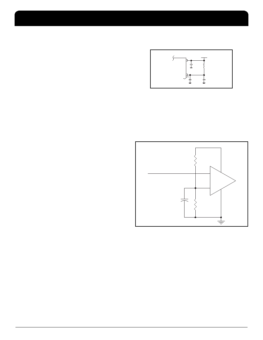
Power Supply Filtering Technique
As in any high speed analog circuitry, the power supply pins are
vulnerable to random noise. To achieve optimum jitter perform-
ance, power supply isolation is required. The ICS87973I-147
provides separate power supplies to isolate any high switching
noise from the outputs to the internal PLL. VDD, VDDA and VDDO
should be individually connected to the power supply plane
through vias, and 0.01F bypass capacitors should be used for
each pin. Figure 2 illustrates this for a generic VDD pin and also
shows that VDDA requires that an additional 10 resistor along with
a 10
F bypass capacitor be connected to the V
DDA pin.
Figure 2. Power Supply Filtering
Wiring the Differential Input to Accept Single Ended Levels
Figure 3 shows how the differential input can be wired to accept
single ended levels. The reference voltage V_BIAS = VDD/2 is
generated by the bias resistors R1, R2 and C1. This bias circuit
should be located as close as possible to the input pin. The ratio of
R1 and R2 might need to be adjusted to position the V_BIAS in the
center of the input voltage swing. For example, if the input clock
swing is only 2.5V and VDD = 3.3V, V_BIAS should be 1.25V and
R2/R1 = 0.609.
Figure 3. Single-Ended Signal Driving Differential Input
VDD
VDDA
3.3V
10
10F
.01F
V_Bias
Single Ended Clock Input
VDD
CLK
nCLK
R1
1K
C1
0.1u
R2
1K
发布紧急采购,3分钟左右您将得到回复。
相关PDF资料
ICS87973DYILFT
IC CLK MULT/ZD BUFFER 52-LQFP
ICS87974CYILF
IC CLK GEN LVCMOS/LVTTL 52-LQFP
ICS894D115AGI-04LF
IC CLK/DATA RECOVERY 20-TSSOP
ICS894D115BGI-01LF
IC CLK/DATA RECOVERY 20-TSSOP
ICS9112AM-17LF
IC BUFFER HI PERFORMANCE 16-SOIC
ICS91305AMILF
IC CLOCK DRIVER LO JITTER 8-SOIC
ICS91305AMLF
IC CLOCK DRIVER LO JITTER 8-SOIC
ICS91309AGILF
IC CLK BUFFER ZD PLL 16TSSOP
相关代理商/技术参数
ICS87973DYI-147LFT
功能描述:IC CLK MULT/ZD BUFFER 52TQFP RoHS:是 类别:集成电路 (IC) >> 时钟/计时 - 时钟发生器,PLL,频率合成器 系列:HiPerClockS™ 标准包装:1,000 系列:- 类型:时钟/频率合成器,扇出分配 PLL:- 输入:- 输出:- 电路数:- 比率 - 输入:输出:- 差分 - 输入:输出:- 频率 - 最大:- 除法器/乘法器:- 电源电压:- 工作温度:- 安装类型:表面贴装 封装/外壳:56-VFQFN 裸露焊盘 供应商设备封装:56-VFQFP-EP(8x8) 包装:带卷 (TR) 其它名称:844S012AKI-01LFT
ICS87973DYILF
功能描述:IC CLK MULT/ZD BUFFER 52-LQFP RoHS:是 类别:集成电路 (IC) >> 时钟/计时 - 时钟发生器,PLL,频率合成器 系列:HiPerClockS™ 标准包装:2,000 系列:- 类型:PLL 频率合成器 PLL:是 输入:晶体 输出:时钟 电路数:1 比率 - 输入:输出:1:1 差分 - 输入:输出:无/无 频率 - 最大:1GHz 除法器/乘法器:是/无 电源电压:4.5 V ~ 5.5 V 工作温度:-20°C ~ 85°C 安装类型:表面贴装 封装/外壳:16-LSSOP(0.175",4.40mm 宽) 供应商设备封装:16-SSOP 包装:带卷 (TR) 其它名称:NJW1504V-TE1-NDNJW1504V-TE1TR
ICS87973DYILFT
功能描述:IC CLK MULT/ZD BUFFER 52-LQFP RoHS:是 类别:集成电路 (IC) >> 时钟/计时 - 时钟发生器,PLL,频率合成器 系列:HiPerClockS™ 标准包装:1,000 系列:- 类型:时钟/频率合成器,扇出分配 PLL:- 输入:- 输出:- 电路数:- 比率 - 输入:输出:- 差分 - 输入:输出:- 频率 - 最大:- 除法器/乘法器:- 电源电压:- 工作温度:- 安装类型:表面贴装 封装/外壳:56-VFQFN 裸露焊盘 供应商设备封装:56-VFQFP-EP(8x8) 包装:带卷 (TR) 其它名称:844S012AKI-01LFT
ICS87974CYILF
功能描述:IC CLK GEN LVCMOS/LVTTL 52-LQFP RoHS:是 类别:集成电路 (IC) >> 时钟/计时 - 时钟发生器,PLL,频率合成器 系列:HiPerClockS™ 标准包装:1,000 系列:- 类型:时钟/频率合成器,扇出分配 PLL:- 输入:- 输出:- 电路数:- 比率 - 输入:输出:- 差分 - 输入:输出:- 频率 - 最大:- 除法器/乘法器:- 电源电压:- 工作温度:- 安装类型:表面贴装 封装/外壳:56-VFQFN 裸露焊盘 供应商设备封装:56-VFQFP-EP(8x8) 包装:带卷 (TR) 其它名称:844S012AKI-01LFT
ICS87974CYILFT
功能描述:IC CLOCK GEN 1-15 PLL 52-LQFP RoHS:是 类别:集成电路 (IC) >> 时钟/计时 - 时钟发生器,PLL,频率合成器 系列:HiPerClockS™ 标准包装:1,000 系列:- 类型:时钟/频率合成器,扇出分配 PLL:- 输入:- 输出:- 电路数:- 比率 - 输入:输出:- 差分 - 输入:输出:- 频率 - 最大:- 除法器/乘法器:- 电源电压:- 工作温度:- 安装类型:表面贴装 封装/外壳:56-VFQFN 裸露焊盘 供应商设备封装:56-VFQFP-EP(8x8) 包装:带卷 (TR) 其它名称:844S012AKI-01LFT
ICS879893AYILF
功能描述:IC CLK GEN LVCMOS/LVTTL 48-LQFP RoHS:是 类别:集成电路 (IC) >> 时钟/计时 - 时钟发生器,PLL,频率合成器 系列:HiPerClockS™ 标准包装:1,000 系列:- 类型:时钟/频率合成器,扇出分配 PLL:- 输入:- 输出:- 电路数:- 比率 - 输入:输出:- 差分 - 输入:输出:- 频率 - 最大:- 除法器/乘法器:- 电源电压:- 工作温度:- 安装类型:表面贴装 封装/外壳:56-VFQFN 裸露焊盘 供应商设备封装:56-VFQFP-EP(8x8) 包装:带卷 (TR) 其它名称:844S012AKI-01LFT
ICS879893AYILFT
功能描述:IC CLK GEN LVCMOS/LVTTL 48-LQFP RoHS:是 类别:集成电路 (IC) >> 时钟/计时 - 时钟发生器,PLL,频率合成器 系列:HiPerClockS™ 标准包装:1,000 系列:- 类型:时钟/频率合成器,扇出分配 PLL:- 输入:- 输出:- 电路数:- 比率 - 输入:输出:- 差分 - 输入:输出:- 频率 - 最大:- 除法器/乘法器:- 电源电压:- 工作温度:- 安装类型:表面贴装 封装/外壳:56-VFQFN 裸露焊盘 供应商设备封装:56-VFQFP-EP(8x8) 包装:带卷 (TR) 其它名称:844S012AKI-01LFT
ICS87993AYILF
功能描述:IC PLL CLK DRIVER 1-5 32-LQFP RoHS:是 类别:集成电路 (IC) >> 时钟/计时 - 时钟发生器,PLL,频率合成器 系列:HiPerClockS™ 标准包装:1,000 系列:- 类型:时钟/频率合成器,扇出分配 PLL:- 输入:- 输出:- 电路数:- 比率 - 输入:输出:- 差分 - 输入:输出:- 频率 - 最大:- 除法器/乘法器:- 电源电压:- 工作温度:- 安装类型:表面贴装 封装/外壳:56-VFQFN 裸露焊盘 供应商设备封装:56-VFQFP-EP(8x8) 包装:带卷 (TR) 其它名称:844S012AKI-01LFT